
PCB processing and handling
- ESD protection
- Solder and solder agents
- Factory equipment
- Personal protective equipment (PPE)
- PCB processing and handling
- Component processing
- Component storage
- SALE

ESD PCB magazine, 563 x 355 x 320 mm
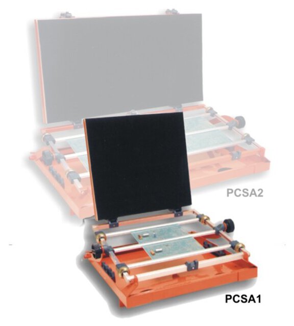
Mounting frame for PCBs, max. 270 x 220 mm
Pressure spring 10 x 63.5 mm, Vaculab
Side panel for ESD PCB magazine
Mounting frame for PCBs, max. 500 x 220 mm
What requirements apply when handling printed circuit boards?
Printed circuit boards must be protected from mechanical stress, contamination and electrostatic discharge. For this reason, electronic assemblies are only touched at the edges where possible and transported in ESD-compliant holders. With assembled PCBs in particular, even low mechanical voltages can damage conductor tracks, solder joints or sensitive components.
Why is ESD protection important when handling PCBs?
Electrostatic voltages can be generated during the transport and processing of PCBs, which can damage semiconductor components. This is why ESD-compliant workstations, transport containers and tools are used. The requirements are based on DIN EN 61340-5-1 and apply in particular to electronics production, test bays and repair workstations.
Which tools are used for PCB processing?
The tools used for PCB processing include depanelling machines, PCB holders, milling systems, cutting tools and PCB handling systems. The selection depends on the material thickness, placement density and separation process. The aim is to achieve reproducible processing with the lowest possible mechanical stress on the assembly.